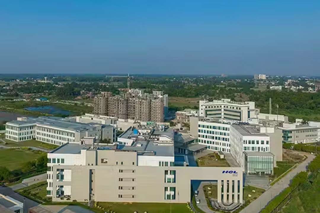
HCLTech has launched its Advanced Semiconductor Lab in Bengaluru with an investment of Rs 185 crore, strengthening its semiconductor engineering capabilities and supporting India’s growing role in the global chip ecosystem. The new facility is designed to accelerate semiconductor innovation, shorten time-to-market for global customers and expand access to integrated testing and post-silicon engineering capabilities.
Spread across 40,000 sq ft the state-of-the-art facility includes 25,000 sq ft of Class 10K and Class 1K cleanrooms. Backed by HCLTech’s two decades of experience in the semiconductor industry, the lab provides end-to-end post-silicon engineering, advanced testing and failure analysis services. It is equipped with advanced semiconductor testing and analytical tools from Teradyne, Advantest, Keysight, Tektronix and Thermo Fisher Scientific Inc.
The facility supports a broad range of activities spanning research and development, pre-production and production qualification. By bringing these capabilities together under one roof, HCLTech aims to enable faster turnaround, improve quality and reduce operational complexity for semiconductor customers worldwide.
The lab is aligned with HCLTech’s Spec2Parts business model, providing an integrated platform covering electrical validation, automated testing, qualification and failure analysis. This approach is intended to streamline the semiconductor development process, helping customers move efficiently from design specifications to finished semiconductor parts.
The Bengaluru facility also addresses critical gaps in India’s semiconductor engineering ecosystem by combining advanced infrastructure with specialised engineering talent. HCLTech said the integrated capabilities will allow customers to access sophisticated testing facilities and technical expertise while reducing the time and complexity involved in semiconductor validation and qualification.
“The inauguration of our Advanced Semiconductor Lab in Bengaluru is a proud milestone for HCLTech and reinforces India’s growing leadership in semiconductor innovation. This facility reflects our deep commitment to investing in high-end engineering capabilities. We are excited to contribute to the country’s vision of becoming a global hub for advanced technology,” said Hari Sadarahalli, Corporate Vice President and Global Head, Engineering and R&D Services, HCLTech.
The investment reflects HCLTech’s continued focus on strengthening high-end engineering and research capabilities in India. Through the new facility, the company aims to support semiconductor companies with comprehensive testing and engineering services while contributing to the development of a stronger and more competitive semiconductor ecosy
TechnoStruct Group is engaged in Building Information Modeling (BIM) and Virtual Design & Construction (VDC) solutions and education. The group operates through TechnoStruct Academy and its wider business operations under TechnoStruct LLC, California, USA, with a presence in the US and India. It provides software, implementation, training and support services for organisations and professionals across the AEC industry.