Yield Engineering Systems (YES), a top supplier of advanced semiconductor processing equipment for AI and high-performance computing (HPC) markets, has announced the receipt of multiple equipment orders from a global frontrunner in AI infrastructure solutions. These orders cover a broad selection of YES’s Dry and Wet processing tools to support panel-level manufacturing on glass substrates for cutting-edge data center and HPC packaging applications. The systems will be integrated into packaging lines designed for hyperscale AI tasks such as training, inference, networking, and co-packaged optics. This partnership highlights the growing industry movement toward glass-based 2.5D and 3D packaging driven by rising demands for system performance, density, and heat management.
YES will deliver a comprehensive suite of advanced equipment designed to support the customer’s panel-level production process with precision, consistency, and scalability. The integrated toolset is engineered to optimize every stage of manufacturing — from material preparation to final finishing — ensuring superior process reliability and production efficiency.
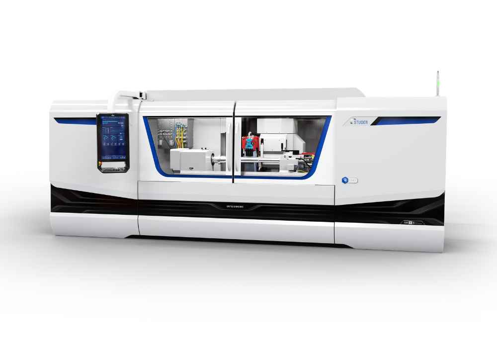
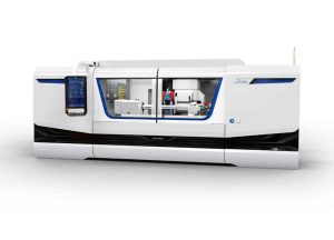
The offering includes the VertaCure™ automated vacuum curing system, which enables complete solvent removal, uniform thermal processing, and exceptional particle control for defect-free results. Complementing this is the VertaPrime™ low-vacuum vapor deposition platform, specifically designed to enhance surface adhesion and prepare panels for subsequent processing steps.
Also featured in the solution set are the VeroFlex™ FAR precision reflow system for consistent interconnect formation, the TersOra™ edge-zone removal platform that delivers accurate and clean edge profiles, and the SURE™ Wet Process Platform, a high-performance wet etching and cleaning solution optimized for large-format panels. Together, these tools provide a robust, end-to-end solution that strengthens yield, quality, and throughput across panel-level manufacturing operations.
Rezwan Lateef, President of YES, commented, “We are thrilled to provide a complete suite of glass panel equipment that supports the shift toward high-volume, panel-level packaging for AI and HPC markets. Our systems have already demonstrated reliability in high-volume production at tier-one integrated device manufacturers and foundries. As the industry embraces larger substrates and co-packaged optics, YES stands out as a trusted partner in both wafer and panel manufacturing ecosystems.”
YC Wong, Vice President of Sales and Business Development at YES Singapore, added, “Glass substrates are gaining traction for next-generation 2.5D and 3D packages due to their stability and electrical advantages. Our strategic presence in Singapore, along with extensive experience in volume manufacturing, enables us to support customers effectively as they transition from traditional wafer formats to panel-based production.”
This order further cements YES’s role as a leader in panel-level packaging technology, addressing critical challenges in curing, cleaning, reflow, and deposition for glass substrates. With AI infrastructure demands accelerating rapidly, YES continues to drive innovation in the next generation of semiconductor packaging.
YES is a prominent provider of advanced material and interface engineering technologies for diverse industries. Its clients include market leaders delivering next-generation solutions across Advanced Packaging for AI and HPC, Memory Systems, and Life Sciences. YES manufactures cutting-edge, cost-efficient production tools for semiconductor packaging, including Vacuum Cure, Coat & Anneal, Fluxless Reflow, Thru Glass Via and Cavity Etch, and Electroless Deposition equipment. Headquartered in Fremont, California, YES is expanding its global footprint to meet growing industry needs.