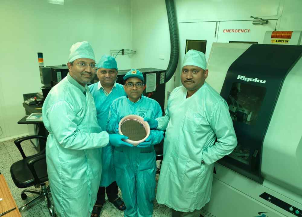
Spintronics AI Semiconductors, a Hyderabad-based semiconductor design and product engineering company, has achieved the first successful wafer-out for its Gallium Nitride-on-Silicon (GaN-on-Si) power High Electron Mobility Transistor (HEMT) development programme. The programme is targeting a device rated at 650 V and 20 A for high-voltage power switching.
The milestone has been achieved through the company’s collaboration with CSIR-Central Electronics Engineering Research Institute (CSIR-CEERI), Pilani. It marks the completion of wafer fabrication and the start of device-level evaluation. Initial wafer-level testing at CSIR-CEERI has produced encouraging preliminary observations.
The testing was conducted under the technical guidance of Dr Pijus Kundu, Senior Scientist at CSIR-CEERI, Pilani. He said, “GaN technology holds immense potential for strengthening India’s strategic semiconductor ecosystem, particularly in high-frequency and high-power applications. The encouraging wafer-testing results represent a significant milestone in the development of indigenous GaN technology, marking an important step towards technological self-reliance and strengthening India’s capabilities in this critical semiconductor domain.”
GaN is a wide-bandgap semiconductor material that enables power devices to operate at higher switching frequencies and with lower losses than conventional silicon-based devices. GaN power HEMTs have potential applications in electric vehicle charging infrastructure, solar inverters, telecommunications, data-centre power supplies, industrial power conversion and energy storage systems. These applications increasingly require higher efficiency and power density.
Raghu Varma, Founder and CEO of Spintronics AI Semiconductors, said, “A wafer-out is the work of many people getting many design decisions right before anything is fabricated. I am proud of what our engineers have achieved, and grateful to our colleagues at CSIR-CEERI. India has the research depth and engineering talent to compete in power semiconductors, and this programme is one way we intend to demonstrate that capability.”
The collaboration between Spintronics AI and CSIR-CEERI was formalised through a Memorandum of Understanding. It brings together the institute’s more than two decades of experience in GaN devices and the company’s semiconductor design, engineering and product-development capabilities. The partnership aims to advance GaN technology and take research and design work towards industry-led product development.
Spintronics AI is also evaluating a proposed GaN semiconductor fabrication facility in Ujjain, Madhya Pradesh. The project is currently at the preliminary feasibility stage and represents a longer-term part of the company’s plans to develop domestic semiconductor manufacturing capabilities.
The GaN-on-Si programme will now proceed to expanded electrical characterisation and reliability assessment. This will be followed by device optimisation, packaging evaluation and product qualification. Further progress and timelines will depend on the technical results.
Srijith Paruchuri, Managing Director of Spintronics AI Semiconductors, said, “Spintronics AI is making strong progress in its indigenous GaN technology development. Our GaN HEMT devices are advancing through detailed characterisation, with this wafer-out an important step in that progress. In parallel, our RF antenna and filter module development programmes are also showing promising results. These milestones reflect our commitment to developing high-performance indigenous semiconductor and RF solutions for Defence, Aerospace, Space and Satellite Communication applications, strengthening India’s capabilities in critical technologies.” The successful wafer-out moves the programme from design and fabrication to hardware evaluation. The results of the next stages will determine the device’s performance and its readiness for further development towards commercial applications.
Founded in 2024 and headquartered in Hyderabad, Spintronics AI Semiconductors Pvt Ltd is an India-focused semiconductor design and product engineering company with expertise spanning architecture, circuit design and verification. Its product roadmap includes GaN power devices, RF power amplifiers, and power-management and protection solutions. The company is also developing indigenous GaN-on-SiC HEMT technology. Spintronics AI works with research institutions, technology partners and industry stakeholders to advance semiconductor technologies from design and development towards commercialisation, with the potential for future domestic manufacturing, subject to technical and commercial feasibility.