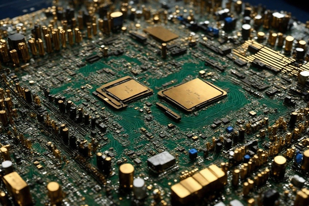
In today’s well-connected, modern, and digital-first world, smartphones, autonomous vehicles, AI infrastructure and even in space exploration and defence, semiconductors are the base of nearly all innovation. They power everything and are now the backbone of modern digital economies.
As the global demand for computing power escalates, nations and industries focus on ensuring a stable, high-quality, scalable semiconductor supply chain. With demand surging, the need for innovation in manufacturing processes is becoming increasingly critical while reducing time to market and cost. Engineering simulations are progressing as a key lever to augment productivity and returns across the value chain of semiconductor manufacturing.
Semiconductor market
The semiconductor industry saw 19% growth in 2024, reaching US$627 billion, with forecasts of US$697 billion this year. It’s on track for US$1 trillion in sales by 2030, potentially reaching US$2 trillion by 2040, driven by 5G, AI, IoT, and electric mobility. Supply chain disruptions and rising design complexity accelerate investments in domestic chip-making capabilities across regions. The US, Europe, Taiwan, Korea, and China have all announced significant incentives to support fabs and chip design. India, too, has many initiatives to build fabs, OSAT facilities, and an indigenous ecosystem. The government has launched the India Semiconductor Mission, or the ISM, with a $10 billion incentive plan to attract global and local investments in chip fabrication, design, display manufacturing, and R&D.
Why focus on semiconductor manufacturing?
Even though India has a solid electronics market, the nation has long depended heavily on imports for key components. Manufacturing is the most capital-intensive stage in the semiconductor value chain. Every step from raw silicon purification to wafer fabrication and packaging must meet benchmarks, including stringent yield, purity, and performance. Engineering choices during design, validation, and scale-up stages directly influence the economics of chip production.
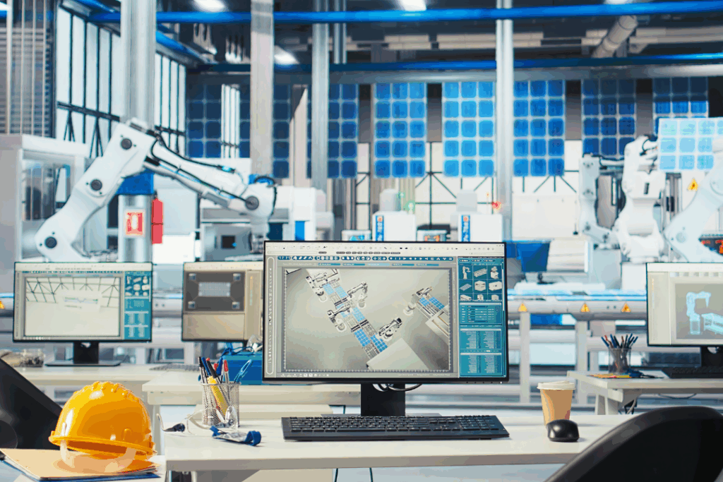
Successful semiconductor manufacturing requires massive scale, precision engineering, and relentless innovation. It also requires advanced tools that reduce guesswork, cut prototype cycles, and simulate real-world physics before a product hits the line.
Semiconductor manufacturing process and engineering challenges across the value chain
The semiconductor value chain is intricate and involves multiple stages.
- Semiconductor Fabrication includes oxidation, etching, doping, deposition, and photolithography.
- Blank Wafer Production, including silicon crystal growth, slicing, shaping, lapping, and polishing.
- Assembly & Packaging that covers die preparation, bonding, molding, and printed circuit board (PCB) integration.
- Testing & Inspection evaluates chip performance under diverse environmental and usage scenarios.
Each of the above stages has its own set of challenges:
- Wafer fabrication involves hundreds of steps, like photolithography, etching, and deposition at the nanometer scale. Even microscopic variances can affect performance or lead to yield losses.
- Packaging and testing require balancing size, thermal dissipation, power, and signal integrity.
- Time to market, cost pressure, yield optimization, and reliability are constant concerns. Key aspects include reducing design cycles, accelerating system validation, and front-loading process decisions.
- Yield Optimization: Controlling wafer contamination, uniform film deposition, and managing process variability is essential.
- Cost Control: Cutting down on prototype iterations, test cycles, and equipment rework. Is key
Fast miniaturization and the push toward 2nm and 3D chip architectures deepen these challenges. A single flaw in deposition uniformity or thermal control can derail yields and impact reliability. Traditional methods are impossible as they often rely on trial and error and are reactive, hence becoming inadequate for today’s nanoscale complexities.
Simulation is a game-changer for semiconductor manufacturing
As devices grow smaller, faster, and more powerful, manufacturing complexities will only deepen. Integrating AI with simulation, high-performance computing, and digital twins is set to revolutionize semiconductor R&D and production. Simulation will, therefore, be vital in optimizing existing processes and enabling innovations in heterogeneous integration, 3D packaging, and sustainable fab operations.
Simulation empowers engineers to virtually prototype and improve every aspect of the semiconductor manufacturing process. These tools provide actionable insights into process performance, failure risks, and system behavior by integrating fluid dynamics, structural mechanics, electromagnetics, and material science.
Here are some key applications of simulation across the value chain:
- Polysilicon Production & Crystal Growth: Simulation augments reactor heating and gas flow for uniform rod growth. This cut prototyping needs and improves the ingot yield.
- Wafer handling processes, such as zipping and chucking, must be accurately simulated to ensure reliable and error-free manipulation of delicate wafers. Additionally, understanding the impact of these processes on wafer warpage is critical for optimizing handling parameters and improving overall yield.
- Wafer dicing is a critical process that directly impacts yield and overall device reliability. To maximize yield, it is essential to optimize the dicing process parameters. Standard techniques include saw dicing and laser dicing, each with unique advantages depending on the application. Given the brittle nature of wafers and the presence of delicate circuitry layers, achieving clean and precise cuts is vital. Thorough validation and testing are required, and simulation plays a key role in understanding and improving the dicing process.
- Die Preparation & Cleaning: CFD models improve wet cleaning efficiency, nozzle design, and particle removal. This leads to faster cycle times and improved cleanliness.
- Thermal Processes (e.g., Heat Treatment, ALD, PECVD): Simulations guarantee temperature uniformity, reduce stress-induced defects, and help fine-tune layer deposition rates.
- Chemical Mechanical Polishing (CMP): High-fidelity models optimize slurry flow and pad contact conditions, ensuring better abrasion performance and reducing material waste.
- Lithography & Etching: Optical and chemical simulations increase mask resolution, predict etch profiles, and lessen reticle iterations, speeding up ramp-to-production.
- Assembly & Packaging: From solder reflow modeling to warpage prediction and moldflow simulation, simulation ensures reliable chip packaging under thermal and mechanical stress.
- Simulations are becoming even more crucial in designing and optimizing advanced ICs like 3DICs. They help engineers analyze mechanical stresses, thermal distribution, and electrical performance across stacked layers, which are more prominent in these complex designs. Simulating material behavior and interconnect performance accelerates the development process and improves the overall performance of 3D ICs.
All these also lead to some measured business impact. There will be a 66% reduction in system validation time. Up to 90% improvement can be seen in operating conditions for better yield, and there will also be up to 10x savings in energy consumption via optimized process controls.
Simulation can thus help manufacturers move from a “build and test” approach to a “simulate and optimize” one. This saves both time and money while improving product quality and consistency.
Future Prospect
Engineering simulations create massive value for chipmakers in this fast-evolving market by addressing yield, time, and cost. Simulation-led engineering is a game-changer in India’s evolving semiconductor ecosystem. Simulation-driven productivity and yield improvements will be crucial for fabs to be globally competitive.
As India builds its semiconductor future, embracing simulation will help overcome barriers. Simulation is not merely a support tool but is vital to semiconductor success.
Disclaimer: This is a guest-authored article. The opinions and information expressed are those of the author alone. Machine Maker does not guarantee the accuracy of the content and assumes no liability for any statements or claims made therein.