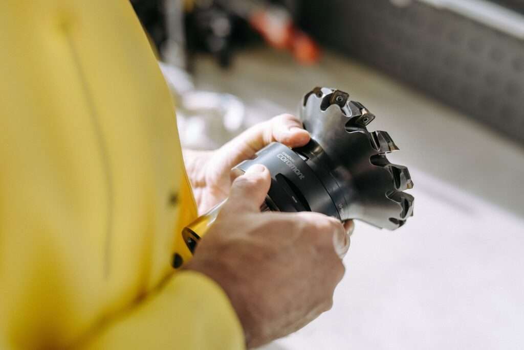
TANAKA Precious Metals has introduced a revolutionary advancement in gold particle bonding technology known as AuRoFUSE™. This groundbreaking innovation facilitates high-density semiconductor mounting through the use of low-temperature fired paste.
TANAKA Precious Metals, a globally renowned company, specializes in the development and production of precious metal products for various industries. With a rich history dating back to 1885, TANAKA has established itself as a leader in the field of precious metals, offering innovative solutions tailored to meet the evolving needs of its customers.
The company’s diverse product portfolio includes materials such as gold, silver, platinum, and palladium, utilized in a wide range of applications spanning electronics, automotive, healthcare, and more. TANAKA’s commitment to research and development ensures continuous innovation, driving advancements in areas like semiconductor packaging, fuel cells, and environmental technologies.
This cutting-edge technique enables the precise mounting of components with a pitch as fine as 4 μm and bumps as small as 20 μm. Such precision caters to the growing demand for miniaturization and enhanced integration in optical and digital devices. This development promises to reshape the landscape of semiconductor manufacturing by offering unparalleled levels of accuracy and efficiency in component assembly.
Presented at the Spring Conference of the Japan Institute of Electronics Packaging, the showcased technology holds promise for achieving greater levels of miniaturization and integration across various chip types. It boasts attributes of low electrical resistance and high thermal conductivity, ensuring robust performance post-mounting in a wide array of applications, including but not limited to LEDs, LDs, smartphones, and automotive components.
The manufacturing process entails several steps, beginning with the metallization of the bonding substrate, followed by the application of photoresist, and concluding with the flow of AuRoFUSE™ into the formed resist frame. Through a meticulous process involving vacuum drying and temporary sintering, AuRoFUSE™ preforms are created, exhibiting minimal deformation and optimal bonding strength for practical usage scenarios.
Conventional methods such as solder-based bonding and electroless plating encounter hurdles in achieving high-density mounting. TANAKA’s innovative approach addresses these challenges by offering low-temperature, low-pressure bonding with exceptional followability on irregular surfaces. The porous nature of AuRoFUSE™ facilitates bonding even in instances of discrepancies in electrode height or substrate thickness.
By precluding fluidity prior to bonding, TANAKA ensures minimal spread and facilitates high-density mounting, heralding a paradigm shift in semiconductor packaging technology. With a strategic plan to disseminate samples and enhance market awareness, TANAKA’s AuRoFUSE™ technology represents a significant leap forward in semiconductor mounting techniques, establishing new benchmarks for efficiency and reliability in cutting-edge technologies.