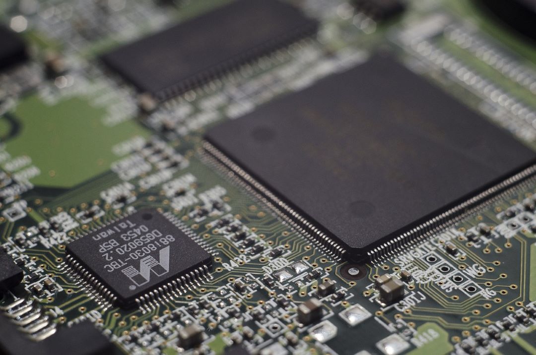
In a significant move towards modernizing the Semi-Conductor Laboratory (SCL) in Mohali, the government has approved a ₹2,000-crore funding plan aimed at enhancing its existing 180-nanometre (nm) chip fabrication line. This initiative marks the beginning of an augmentation process that will introduce new tools, replace outdated equipment, and eliminate inefficiencies in the chip manufacturing process.
The upgrade is expected to attract global companies like Applied Materials, Cadence, and Synopsys, which specialize in semiconductor tools and machinery. With it is expanding its operations to include design startups for limited chip production, officials emphasize the need to reduce project delivery times for chip manufacturing. Currently, SCL incurs approximately ₹127 crore annually on equipment repair and maintenance, primarily due to the age of its existing machinery.
Plans are also underway to upgrade it’s chip technology to higher nodes, such as 65 nm, 40 nm, and 28 nm, with the Ministry of Electronics and IT (MeitY) poised to invite proposals from potential technology partners to facilitate this upgrade.
Additionally, the government aims to increase the quantity of chips produced at SCL by 50 to 100 times as part of its restructuring strategy. This may also involve reorganizing teams to establish a dedicated business development unit focused on addressing industry and startup needs.
The approved ₹2,000-crore funding is part of a broader ₹76,000-crore semiconductor incentive scheme. Previously, the government allocated $1 billion (approximately ₹8,000 crore) for SCL’s modernization, with the total investment likely to increase as the initiative seeks to elevate SCL to global standards while supporting research and development, prototyping, and capacity expansion.
Officials have noted that performance, pricing, and cycle time are critical factors in semiconductor processes. SCL currently lags behind global foundries, which typically have a cycle time of about three to four months. Analysts suggest that leveraging SCL for commercial purposes is vital, as startups often turn to established players like TSMC and GlobalFoundries for even limited chip samples, incurring substantial costs and facing challenges in testing and manufacturing.
As chip technologies evolve, many startups are now focusing on 28 nm technology or lower. The SCL needs to adapt by shifting to these lower nodes, as its current 180 nm technology has limited potential. SCL operates two fabrication lines for 6-inch and 8-inch wafers, alongside an ATMP unit and a compound semiconductor unit.
To support the construction of a new fab unit, SCL is currently exploring land acquisition near its existing facility, with potential land valued at around ₹250 crore. Discussions regarding the acquisition are ongoing.