KASFAB Tools Private Limited, a KAS Group company under UHP Technologies and KASTECH Equipment, has inaugurated India’s first manufacturing facility for semiconductor equipment catering to global clients The state-of-the-art facility in Doddaballapur was inaugurated today in the presence of global supply chain partners and representatives from Fortune 100 companies. The event was graced by Dr Suraj Rengarajan, Head of Semiconductor Products Group at Applied Materials India, Dr. Ankineedu Velaga, SVP & Country Head of YES India, and Prof. Srinivasan Raghavan, Chairman of CeNSe, IISc, who formally opened the facility.
KAS Group, a prominent engineering leader with a robust portfolio including UHP Technologies and KASTech Equipments, has a proven track record of serving the solar and semiconductor industries. Their expertise spans solar fabs and semiconductor R&D facilities. Recently, UHP Technologies secured a significant contract with Micron Semiconductor Gujarat, further bolstering the Group’s position in the industry.
This groundbreaking initiative marks a pivotal milestone in India’s journey toward self-reliance and global leadership in semiconductor manufacturing. KAS Group plans to invest heavily in its newly established company, KASFAB Tools Private Limited, starting with INR 20 crore in the initial phase and an additional INR 250 crore in subsequent expansion. With a focus on tapping into a USD 25 billion global market, the Indian semiconductor ecosystem is projected to reach INR 2,500 crore in the next 3–5 years. Revenue for FY 2025-26 is forecasted at INR 50 crore, with exponential growth anticipated as the company scales further.
“This world-class facility represents a major step forward in strengthening India’s semiconductor ecosystem,” said Mr. Manjunath Jyothinagara, Managing Director of KASFAB Tools Pvt. Ltd. “By providing advanced manufacturing capabilities, we are not only supporting global customers but also positioning Karnataka as a hub for innovation and high-tech engineering. This initiative will create jobs, attract significant investments, and accelerate India’s ambitions to become a global leader in semiconductor manufacturing.”
“With India’s first-of-its-kind infrastructure capable of supporting industry giants, we are excited to collaborate with companies like Applied Materials, LAM Research, Tokyo Electron, and Yield Engineering Systems. As global semiconductor equipment manufacturers diversify their supply chains, India offers a compelling opportunity for contract manufacturing. With its vast talent pool and engineering ecosystem, India is poised to drive MSMEs to confidently participate in building a vibrant local semiconductor ecosystem,” he added.
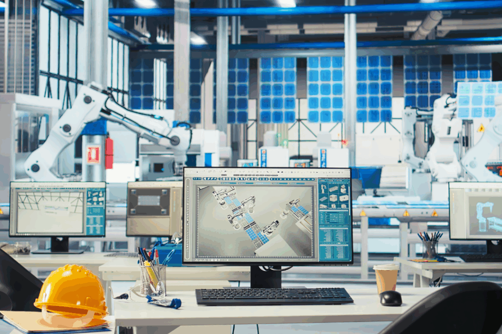
The facility, sprawling across 20,000 sq. ft. on the outskirts of Bangalore, was developed after extensive benchmarking of similar setups in the USA, Japan, South Korea, Malaysia, and China. It is one of the most advanced facilities of its kind in India. Equipped with cutting-edge infrastructure, it includes Class 10 and Class 100 cleanrooms, high-precision welding for plastics and metals, component fabrication, and ultrasound-aided cleaning using deionized (DI) water.
Additionally, the facility houses independent test and validation tools, a safety simulation bench, and functional testing capabilities, all designed to meet the highest global standards. Its pioneering features include precision welding, comprehensive testing setups, and cleanrooms, enabling it to meet the demands of leading global customers like Applied Materials, LAM Research, Tokyo Electron, and Yield Engineering Systems. This initiative underscores India’s growing importance in the global semiconductor landscape, leveraging advanced infrastructure to attract collaborations and drive innovation in the high-tech sector.