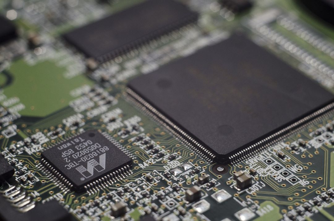
The Government of India has approved 23 semiconductor design projects under the Design Linked Incentive (DLI) Scheme to strengthen the nation’s capabilities in chip development. The projects, led by domestic startups and MSMEs, aim to deliver indigenous chips and System-on-Chip (SoC) solutions for applications including surveillance, smart energy, microprocessors, and networking. So far, 72 companies have gained access to advanced Electronic Design Automation (EDA) tools to support their design efforts.
Among the approved participants, Vervesemi Microelectronics, a fabless semiconductor company, announced its upcoming range of advanced integrated circuits designed to enhance India’s self-reliance in semiconductors and strengthen global competitiveness. Founded in 2017, Vervesemi is one of the first Indian companies to export semiconductor intellectual property (IP) worldwide. Its proprietary machine learning–driven analog chain IPs are already embedded in products by leading international manufacturers.
The company’s portfolio includes over 110 IPs, 25 IC SKUs, 10 patents, and 5 trade secrets, powering applications in space, defense, industrial automation, and smart energy. As an early participant in both the Design Linked Incentive (DLI) Scheme and the Chips to Startup (C2S) program, Vervesemi is building chips designed in India to reduce dependence on imports and promote innovation.
Vervesemi is advancing a suite of application-specific integrated circuits (ASICs) designed for high-reliability environments, with engineering samples expected to roll out between late 2025 and 2026. These upcoming chips are aimed at critical sectors such as electric vehicles, aerospace, industrial automation, and smart energy systems.
Notable developments include a BLDC Controller ASIC, created under the C2S Programme, to power compact motor applications in appliances and fans, with sampling planned for 2026. Also slated for 2026 is a Precision Motor-Control ASIC, recognized under the Design Linked Incentive (DLI) scheme, catering to demanding applications in EVs, drones, and automation systems.
In the aerospace domain, Vervesemi is developing a Data Acquisition ASIC enhanced with AI capabilities, purpose-built for mission-critical space and avionics operations, with samples targeted for 2026. Meanwhile, the company is also preparing to release a Weighing Scale & Bridge Sensor ASIC by the end of 2025, optimized for advanced weighing solutions and force-touch sensing. Complementing this is the Smart Energy Metering ASIC, designed for ultra-accurate, multi-channel measurements in next-generation smart grid infrastructure, also sampling by the end of 2025.
Vervesemi integrates machine learning into its ICs, enabling self-healing systems, fault tolerance, and predictive diagnostics. These capabilities boost reliability, energy efficiency, and yield, setting new performance benchmarks in semiconductor design.
“These innovations mark a defining moment for India’s semiconductor ecosystem,” said Rakesh Malik, Founder & CEO of Vervesemi. “By delivering high-performance ICs made in India, we are reducing import reliance while demonstrating global leadership in chip design.”
“Our signal-chain expertise combined with machine learning enables adaptive calibration and predictive diagnostics, creating ICs that push boundaries of precision and efficiency,” added Pratap Narayan Singh, Founder & CTO of Vervesemi. “India’s vision is to lead the world in semiconductor design—where every device carries a designed-in-India chip,” said Sunita Verma, Group Coordinator (R&D), MeitY.
Vervesemi Microelectronics is a fabless semiconductor firm specializing in analog IPs and ASICs. With designs spanning five foundries and more than 20 technology nodes, Vervesemi delivers up to 10x improvements in performance, power, and area. Its solutions are trusted globally across 5G, Wi-Fi 6/7, energy, motor control, aerospace, and industrial applications.


