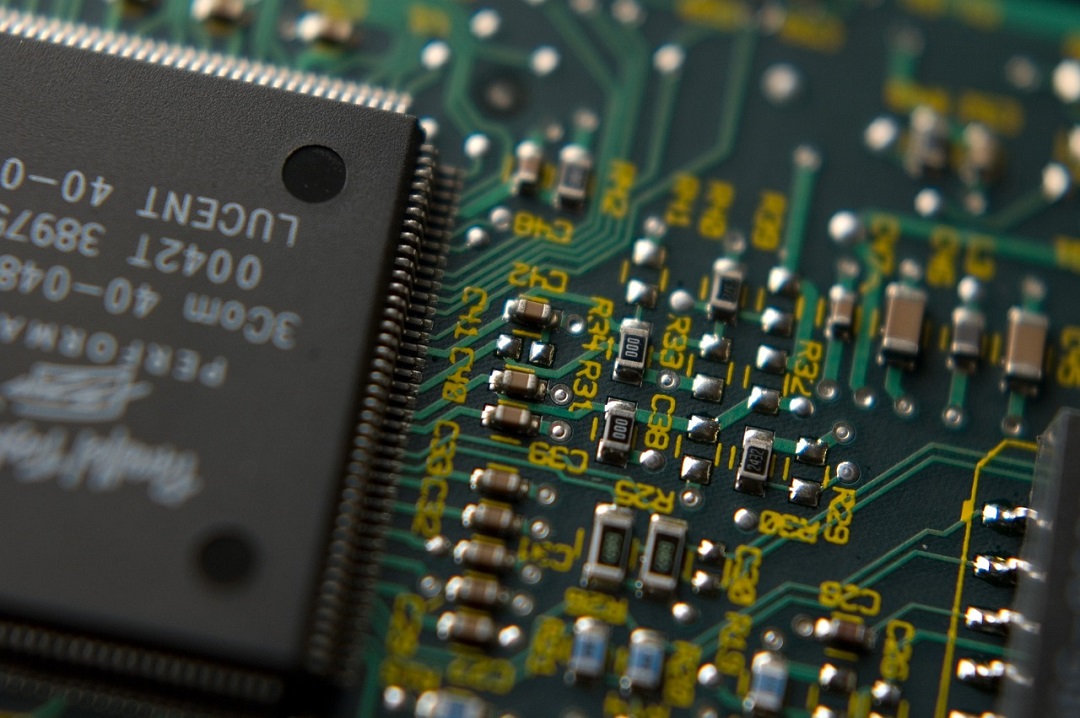
HCLTech, a leading global technology provider, has been named a Design Solution Partner (DSP) within Samsung’s Advanced Foundry Ecosystem (SAFE™). This collaboration aims to drive innovation in semiconductor development by leveraging HCLTech’s expertise in engineering and R&D services.
Through the SAFE™-DSP program, HCLTech will offer integrated circuit (ASIC) design services tailored to semiconductor clients looking to use Samsung’s cutting-edge process technologies. As part of the partnership, Samsung will provide advanced technology training for HCLTech employees, offer technical support for end-to-end projects, and improve wafer access through Multi-Project Wafer (MPW) programs to streamline prototyping and production.
Taejoong Song, Vice President and Head of the Technology Planning 2 Team at Samsung Electronics, shared, “HCLTech’s expertise in India and its global experience with SoC platforms and IP partnerships are vital for advancing the next wave of silicon technologies. This partnership strengthens our commitment to innovation and speeds up the development of new semiconductor solutions.”
Sanjay Gupta, Corporate Vice President of North Asia at HCLTech, added, “The semiconductor industry is rapidly growing, and our partnership with Samsung Foundry underscores our focus on creating innovative, custom silicon solutions. By combining HCLTech’s and Samsung Foundry’s strengths, we aim to accelerate advancements in semiconductor technology and meet the evolving needs of the global market.”
HCLTech, with over 220,000 employees across 60 countries, is a global leader in digital, engineering, cloud, and AI services. The company’s services span across multiple industries, including financial services, manufacturing, life sciences, healthcare, technology, telecom, retail, and public services. For the 12 months ending December 2024, HCLTech reported consolidated revenues of $13.8 billion.